Category Archives: Hardware_knowledge

Linux GPIO(2) – IMPLEMENT and ACCESS EXPANDED gpio

drivers/gpio/gpio-pca953x.c is a driver for tca9539 and similar TI I2C I/O expander.

In the function pca953x_probe(),

  • set up the list of the callback functions (direction_output() etc), and other properties, such as base, ngpio.
  • register the gpio chip via gpiochip_add_data().

In the probe function of max9286 driver,

  • read the device tree line “pwdn-gpios = <&tca9539 2 0> “

sensor->pwdn_gpio = devm_gpiod_get_optional(&client->dev, “pwdn”, GPIOD_IN);

  • power on max9286: gpiod_direction_output(sensor->pwdn_gpio, 1);

Note:

driver/gpio/gpiolib.c is the core of GPIO implementation.

  • A new GPIO chip registers itself via calling the function gpiochip_add_data();
  • the gpio calls from users, such as gpiod_get(), gpiod_direction_output(), goes here first, then the chip-registered callback functions will be invoked.
  • devm_gpiod_xx() functions are resource-managed version of gpiod_xx() functions.

For more details, refer to General Purpose Input/Output (GPIO) — The Linux Kernel documentation

I2C(2) — QNX implementation

There is a resource manager interface, for applications to access a master. The resource manager layer registers a device name (usually /dev/i2c0).

Interface between applications and resmgr:  devctl() commands, such as

  • DCMD_I2C_SEND It executes a master send transaction and returns when the transaction is complete.
  • DCMD_I2C_RECV command executes a master receive transaction. It returns when the transaction is complete.
  • DCMD_I2C_SENDRECV command executes a send followed by a receive. This sequence is typically used to read a slave device’s register value. When multiple applications access the same slave device, it is necessary to execute this sequence atomically to prevent register reads from being interrupted.

A typical one-byte write function in an application:

struct send_recv
{
    i2c_send_t hdr;
    uint8_t buf[2];
} i2c_data;
	int error = EOK;

	i2c_data.buf[0] = reg_addr;
	i2c_data.buf[1] = data;
	i2c_data.hdr.len = 2;
	i2c_data.hdr.slave.addr = slave_addr;
	i2c_data.hdr.slave.fmt = I2C_ADDRFMT_7BIT;
	i2c_data.hdr.stop = 1;

	error = devctl(fd, DCMD_I2C_SEND, &i2c_data, sizeof (i2c_data), NULL);

A typical one-byte read function in an application:

struct send_recv
{
    i2c_sendrecv_t hdr;
    uint8_t buf[2];
} i2c_data;

int error = EOK;
int retry, timeout = 10;

i2c_data.buf[0] = reg_addr;
i2c_data.hdr.send_len = 1;
i2c_data.hdr.recv_len = 1;
i2c_data.hdr.slave.addr = dev_addr;
i2c_data.hdr.slave.fmt = I2C_ADDRFMT_7BIT;
i2c_data.hdr.stop = 1;
error = devctl(fd, DCMD_I2C_SENDRECV, &i2c_data, sizeof (i2c_data), NULL);

Interface between resource manager and the hardware driver: a list of functions.

  • upon receiving DCMD_I2C_SEND, resmgr calls h/w function send().
  • upon receiving DCMD_I2C_SENDRECV, resmgr calls .send() first, then .recv() function.

I2C hardware driver implements the list of functions. The implementation is h/w dependent. The description below is an example which is done for a specific I2C controller.

  • .send function
    • send the slave address to the bus via a few out32()s .
    • wait for ACK (could be an interrupt).
    • send the register address to the bus via out32() calls.-— buf[0]
    • wait for ACK (could be interrupt).
    • send each data byte to the bus via out32() calls. — buf[1], buf[2],,
    • wait for ACK (could be interrupt).
  • . recv function
    • send the slave address to the bus: a few out32()s.
    • wait for ACK (could be an interrupt).
    • initiate READ via out32() for each byte requested.
    • wait for the READ done.

More about the implementation

  • The resmgr is single-threaded, and each DCMD is handled in a synchronized way (returns until the requested transaction is complete) . As a result,
    • when multiple applications try to access different I2C slaves, respectively, at the same time, there is no issue — the DCMD commands are taken care of one by one, without being interrupted by others.
    • when multiple applications try to access the same I2C slave at the same time, although the individual command can be done without interruption, there could be race conditions. This needs to be avoided.
  • The existing resmgr and i2c drivers only work in single-thread resmgr environment. If there are multiple threads handling CDMD commands, it will be a total mess..
    • DCMD_I2C_SEND/RECV leads to a send or receive transaction. Although the transaction in the physical level can be considered “atomic”, the implementation in resmgr and h/w driver is not atomic at all: there are quite some lines of code, there are a few calls to out32()s, and most critically, there is no mutex or other protections in either resmgr or driver.
  • If there are multiple masters, a separate instance of the resource manager should be run for each master.
    • the option ‘c’ looks for this purpose: ‘c’ is used to specify the number of threads. once specified, each thread will start a resource manager.
    • in this case, although the arbitration is supported in the physical layer, some synchronization will be needed between different master/resmgr.

One use case of fixed-point number — image scaling

One of the image processing procedures is scaling — to resize the original picture to be bigger or smaller. if this is done by a hardware block, usually the software needs tell the hardware about the resizing details:

  1. provide the original picture size and the scaled size only. This is easy for the software, while the hardware needs figure it out by itself which filter (if there are a few) it needs to use in order to achieve the goal.
  2. provide more information, other than just the original size and scaled size. For instance, provide the scaling ratios for each filter which might be involved. When doing this, the software usually need provide a fixed-point scaling ratio value which will be stored in one register.

The background of this scenario

  • The hardware performs only down-scaling, up to the scaling ratio 8.
  • there is a decimal filter available, which can do the scaling ratio 2,4,8.
  • a bilinear filter can handle a maximum scaling ratio 2.

The hardware provides 2 register fields per direction (horizontal, vertical) for the software to set the scaling ratio.

1) DEC_RATIO 2-bit field, it controls the pre-decimation filter.

00b – Pre-decimation filter is disabled.
01b – Decimate by 2
10b – Decimate by 4
11b – Decimate by 8

2) SCALE_FACTOR 14 bit fixed-point, with 12 fractional bits. This scale factor will be provided to bilinear filter.

How does it work

Assume the original size is 1280 and we need scale it down to 256 or 284.

(1) 256

The scaling ratio is 1280/256 = 5.

We need set 4 to DEC_RATIO.

We need set 5/*4 = 1.25 to SCALE_FACTOR.

(2) for 284

The scaling ratio is 1280/284 = 4.50704…

We need set 4 to DEC_RATIO.

WE NEED SET 4.5/4 = 1.12676 to SCALE_FACTOR.

How do we program it

uint32_t width;

uint32_t scaling_width;

(1) DEC_RATIO

uint32_t dec_ratio;

dec_ratio= width / scaling_width; // note we need validate if dec_ratio < 16.0

Then we need find a way to map dec_ratio the DEC_RATIO field. There could be done by using some math, or just an array for mapping since there are no many numbers involved.

static const uint8_t dec_array[] = {0, 0, 1, 1, 2, 2, 2, 2, 3};

if (dec_ratio > 8) {

dec_ratio = 8;

}

write dec_array[dec_ratio] to DEC_RATIO field.

(2) SCALE_FACTOR

(2.1)If the hardware doesn’t have specific requirement about rounding, we simply calculate scale_factor as below.

uint32_t scale_factor;

scale_factor = (width * (1 << 12) )/( scaling_width * (2 << dec_array[dec_ratio]));

// note that the calculation above avoids the floating-point math, so it is faster than calculation below and the result is same.

scale_factor = (uint32_t)((float) width/( scaling_width * (2 << dec_array[dec_ratio])) * (1 << 12);

(2.2) If the hardware wants to round the number to a nearest higher integer, a bit complicated math is needed here, we can either simply use ceil() function, like

float scale_factor;

scale_factor = ((float) width/( scaling_width * (2 << dec_array[dec_ratio])) * (1 << 12);

scale_factor = ceil(scale_factor);

then set (uint32_t)scale_factor to SCALE_FACTOR field.

or we can use fixed-point math to achieve the same result, with floating-point math avoided, as blow.

#define NUM_EXTRA_BITS 4

uint32_t scale_factor;

scale_factor = width * (1 << (12 + NUM_EXTRA_BITS) / (scaled_width * (2 << dec_array[dec_ratio]));

scale_factor = (scale_factor + (1 << NUM_EXTRA_BITS) – 1) >> NUM_EXTRA_BITS;

I2C (1) — how it works

History

I2C (inter IC) was invented by Philips Semiconductor (now named NXP). It is typically used to attach low-speed peripherals to processors/micro-controllers. Since 2006, no licensing fees are required to implement I2C protocol, but fees are still required to obtain I2C addresses, allocated by NXP.

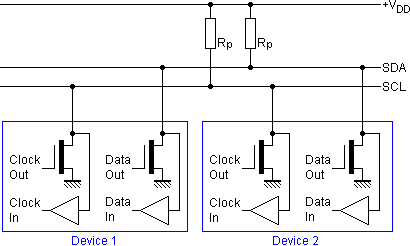
I2C bus (SDA, SCL)

  • bidirectional
    • both outputting and inputting signals on the wire are possible (it can sense the voltage level of the wire).
  • open-drain, or open-collector
    • masters and slaves can only drive these lines low, or leave them open;
    • each line requires a pull-up resistor on it, to pull the line up to VCC, if no I2C device is pulling it down.

i2c_interface

more on pull-up resistor:

  • without a pull-up resistor, he device is not able to generate the I2C start condition.
    • sometimes, there is no external pull-up, but an internal pull-up can be enabled.
    • lack of pull-up will not damage either IC, as PNP transistor is being used.
  • resistor selection: start with 4.7K, and adjust down if necessary.
    • note: a small resistor might be too weak for I2C pull up (it might still work, depending on the I2 speed, etc).

I2C bus transaction

A master is the device which initiates a transfer, generates clock signals and terminates a transfer. A slave is the device addressed by a master.

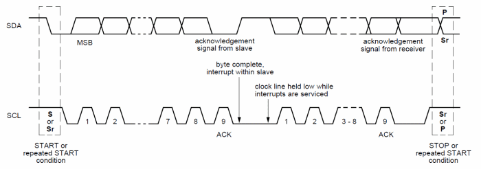
  • all transactions begin with a START and are terminated by a STOP.
    • A HIGH to LOW transition on the SDA line while SCL is HIGH defines a START condition.
      A LOW to HIGH transition on the SDA line while SCL is HIGH defines a STOP condition.
  • Usually, slaves are in the idle condition, monitoring the SDA and SCLK lines for the start condition and the correct address.
  • Following the start condition, the 8 address bits are transferred  (one bit per clock cycle).
  • The slave,
    • responds by pulling the data line low during the ninth clock pulse( this is known as an acknowledge bit) if it recognizes its address, or
    • not-acknowledges(NACKs) the master by letting SDA be pulled high (come ack to the idle condition) if it is not its address.
  • Byte format. Every byte put on the SDA line must be eight bits long. The number of bytes that can be transmitted per transfer is unrestricted. Each byte must be followed by an Acknowledge bit. Data is transferred with the Most Significant Bit (MSB) first .

data-transfer

below shows an example of writing/read a single byte to/from a slave device (slave 7-bit address: 010000xb). Gray color means master controls SDA line while while color indicates slave controls SDA line.

write

read

NOTE:

  1. A read contains 2 bus transactions: the first one is used to send the register address (R/W bit is 0 for this one ); the future one(s) are used to receive data ( R/W bit is 1 in this case).
  2. for writes, the slave sends an ACK after every data byte is successfully received; for read, the master usually sends an ACK after every data byte is received. When the master wants to stop reading, it sends a NACK after the last data byte, to create a STOP condition on the bus.

I2C Arbitration and collision detection

Several I2C multi-masters can be connected to the same I2C bus and operate concurrently. By constantly monitoring SDA and SCL for start and stop conditions, they can determine whether the bus is currently idle or not. If the bus is busy, masters delay pending I2C transfers until a stop condition indicates that the bus is free again.

However, it may happen that two masters start a transfer at the same time. During the transfer, the masters constantly monitor SDA and SCL. If one of them detects that SDA is low when it should actually be high, it assumes that another master is active and immediately stops its transfer. This process is called arbitration.

Probed signal examples

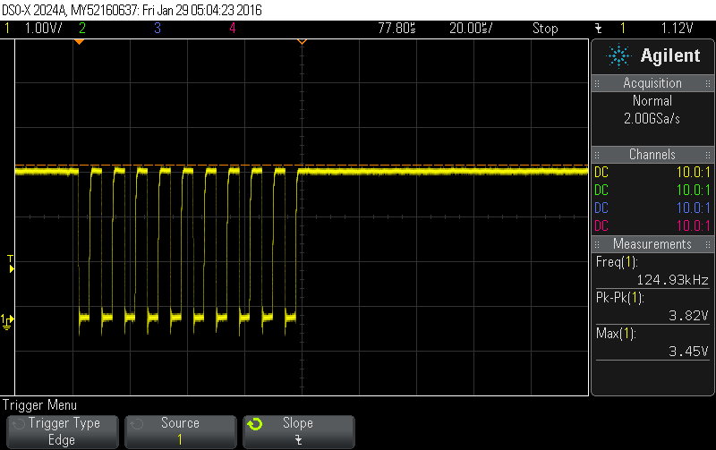
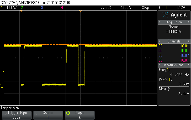
Example #1: (the slave 0x70 doesn’t respond)

# irecv -n/dev/i2c0 -a0x70 -l1  //  0111 0000 –> 1110 0001 DCMD_I2C_SENDRECV, send STOP.

i2c0_SCLi2c0_SDA

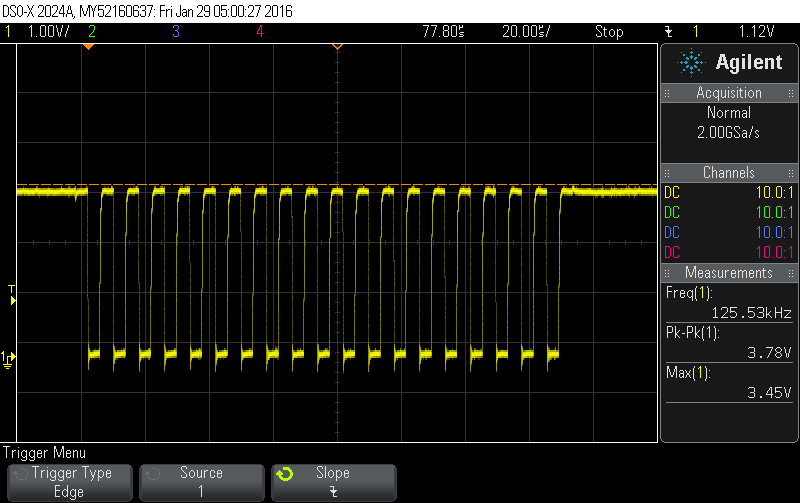
example #2 (the slave 0x6c works well)

# irecv -n/dev/i2c4 -a0x6c -l1   // 0110 1100 –> 1101 1001   DCMD_I2C_SENDRECV, send STOP, too.

Data recvd: 15h  // 0001 0101

i2c4_SCLi2c4_SDA

Circuit basics(6):pull up & pull down

The purpose of pull up/down is to insure that a circuit has a default value (high, or low), given no other input:

a pull up resistor (connect to a power supply) pulls the line high;

a pull down resistor(connect to ground) pulls the line down.


Pull-up resistor                                    pull-down

http://www.seattlerobotics.org/encoder/mar97/basics.html

 Example
MON_INT_N[2] is connected to OM5_GPIO8_233. INT2 pad can be configured as active high; GPIO is configured as input (internal pull up/pull down disabled; high level detection).
open_drain_2 open_drain_1
 When MON drives 3.3V (high), the downside of R14130, closer to MON, is 2.5V due to 1.8V (R13993) pull-up.
Note: INT2 pad can be configured to open-drain, too. I assume that the “NB” resisters are there, in case the pad is configured as open drain?


Circuit Basics (5): Open drain

An alternate to tri-state logic is open drain output:

  • the output signal is applied to the base of an internal NPN transistor.
    • it controls the transistor switching.
  • The emitter is grounded internally.
  • The real output will be on the collector — open collector (the output is taken from between the collector and the emitter).  The output would be either
    • low, when the transistor is on, as the output is forced to nearly 0 volt; or
    • nothing (no current flows), also called “high-Z”, high impedance, when the transistor is off.

opendrain

In practice, a pull-up or pull-down resistor is required, to keep the digital output in a defined logic state. An external pull-up resistor can be used to raise the output voltage when the transistor is turned off.

The advantage of open drain circuit:

  • all the devices can pull the signal line low, but can not drive it high.
    • avoid conflicts where one device drives the line high, while another tries to pull it low.
    • inactive devices would not try to hold the line high.
    • pull up resistor can be external, no need to be connected to the chip supply voltage.

Circuit basics(4): three-state logic

High impedance (hi-Z, tri-stated, floating) means the output is not being driven to any defined logic level (neither logical high, nor low).

The use of high impedance: allow multiple circuits to share the same output line. When you enable the output (pull the line OE to low, or write to a reg), the output will drive it respective loads (0, or 1). Otherwise, it is in high-impedance.

  • A pull-up resistor can be used to try to pull the wire to high and low voltage levels. When devices are inactive, they tri-state their outputs. When all the devices on the bus have done this, the pull-up resistor will pull the line up. If a dvice wants to communicate, it drives the line low.
Example
the device document says it “employs high-impedance CMOS on all signals pins. Voltage on any signal pin that exceeds the ranges can induce destructive latch-up (a type of short circuit in IC)”.
All BT656_D(x) pins are connected to imx_CSI1_DAT(12~19). At the rightmost, it is 3V3DC connected. The decoder uses 3.3V, 1.8V.
sch_1
shc_3
To pull the line/pin in a defined status/level when there is no signal output,
  • For non-used pins (maybe used by other component), e.g MX_CSI1_DAT(1), R10845 is NB (for pull down), R10872 is 4K7(pull up), which effectively pull up the line (3.3V).
  • For pins being used: MX_CSI1_DAT(12), R10184 is 10K,
    • which effectively pulls down the line when there is no signal coming;
    • when the device outputs signals (drive 3.3V or 1.8V on the pin), the line will be high???

Circuit basics (3) — Transistor example

State of Transistor
  •  If there is zero current though it, the transistor is in “CUTOFF” state.
  • If there is maximum current through it, called “saturation”.
  • Anywhere between saturated and cutoff is called “active” mode.
transistor_3
An example of common Emitter
transistor_6
1. Solar cell serves as a light sensor: by using a solar cell to provide 1V (> 0.7V),
  • With the solar cell darkened, the transistor behave as an open switch between collector and emitter.
  • When the solar cell is powered, electrons will flow from the emitter through to the base, up to the left side of the lamp, back to he positive side of the battery —A closed switch
2. Common emitter can e used to produce an output voltage derived from the input signal, rather than a specific output current.
transistor_7 
  • With the solar cell darkened, the transistor behave as an open switch between collector and emitter. there is maximum voltage drop between collector and emitter.
  • When the solar cell is fully powered, minimum voltage drop between collector and emitter.
Note:
  • For an amlifier to work properly, it must be biased on on the time (not just when a signal is present).
    • “On” means current is flowing through the transistor (VB = 0.6 ~ 07V). Usually, a CD circuit is used to achive the biasing.
Common emitter:

Circuit Basics (2)– transistor

Bipolar transistor consists of two PN-junctions — two diodes back to back.
How it works: when you apply a small current to the base (from emitter to base, for NPN type), a much larger current can flow through the transistor (from emitter to collector, for NPN type)
3 leads/legs:
  • emitter,
  • base,
  • collector.
    • One of them is usually grounded.

transistor_1

transistor_2

The choice between NPN and PNP is really arbitrary: all that matters is that the proper current directions are maintained.
Some rules:
  • To get transistors to work,
    • For NPN, collector must be more positive in voltage than emitter.
    • For PNP, collector must be more negative in voltage than emitter.
  • IB + IC = IE,
    • IC is almost equal to IE, as the base current is very small.
  • IC = bIB, b is called the current gain, typically 20 ~ 200
    • Base(small) current is the only current that goes through the base wire of the transistor.
    • Collector(large)current is the only current that goes through the collector wire of the transistor.
    • emitter current is the sum of the base and collector current.

Circuit bacics (1)– Diode

diode

Diode blocks current in one direction while letting current flow in another direction.
 junction diodes are common: put a pice of N type silicon next to a piece of P type silicon.
  • N material has excess negative charge (electrons);
  • P material has excess positive material (holes).
Characteristics:
  • Diode is forward biased when Vanode > Vcathode (usually 0.7Volts, needed to start the hole-electron combination process at the junction).
    • Conducts current strongly.
    • Voltage drop across diode is (almost) independent of diode current.
    • Effective resistance (impedance) of diode is small.
  • Diode is reverse biased when Vanode < Vcathode.
    • Conducts current very weakly (perhaps 10 microamps)
    • Diode current is (almost) independent of voltage, until breakdown (the junction breaks down and lets current through if you apply enough reverse voltage).
    • Effective resistance (impedance) of diode is very large.
Useful links: