Circuit Basics (5): Open drain

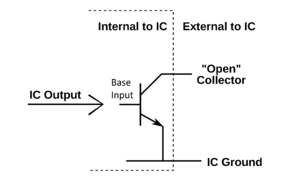
An alternate to tri-state logic is open drain output:

  • the output signal is applied to the base of an internal NPN transistor.
    • it controls the transistor switching.
  • The emitter is grounded internally.
  • The real output will be on the collector — open collector (the output is taken from between the collector and the emitter).  The output would be either
    • low, when the transistor is on, as the output is forced to nearly 0 volt; or
    • nothing (no current flows), also called “high-Z”, high impedance, when the transistor is off.

opendrain

In practice, a pull-up or pull-down resistor is required, to keep the digital output in a defined logic state. An external pull-up resistor can be used to raise the output voltage when the transistor is turned off.

The advantage of open drain circuit:

  • all the devices can pull the signal line low, but can not drive it high.
    • avoid conflicts where one device drives the line high, while another tries to pull it low.
    • inactive devices would not try to hold the line high.
    • pull up resistor can be external, no need to be connected to the chip supply voltage.
Circuit basics(4): three-state logic

High impedance (hi-Z, tri-stated, floating) means the output is not being driven to any defined logic level (neither logical high, nor low).

The use of high impedance: allow multiple circuits to share the same output line. When you enable the output (pull the line OE to low, or write to a reg), the output will drive it respective loads (0, or 1). Otherwise, it is in high-impedance.

  • A pull-up resistor can be used to try to pull the wire to high and low voltage levels. When devices are inactive, they tri-state their outputs. When all the devices on the bus have done this, the pull-up resistor will pull the line up. If a dvice wants to communicate, it drives the line low.
Example
the device document says it “employs high-impedance CMOS on all signals pins. Voltage on any signal pin that exceeds the ranges can induce destructive latch-up (a type of short circuit in IC)”.
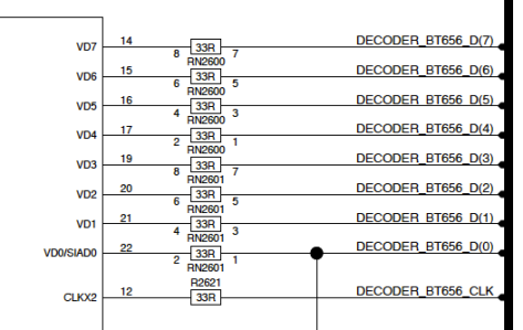
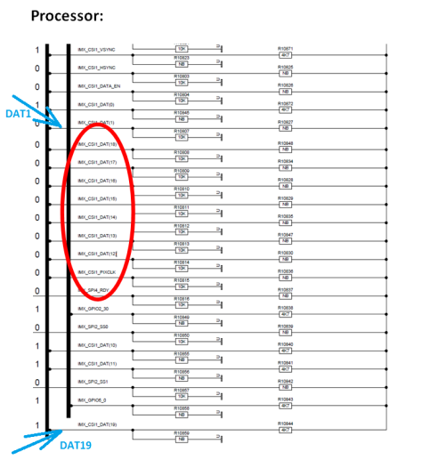
All BT656_D(x) pins are connected to imx_CSI1_DAT(12~19). At the rightmost, it is 3V3DC connected. The decoder uses 3.3V, 1.8V.
sch_1
shc_3
To pull the line/pin in a defined status/level when there is no signal output,
  • For non-used pins (maybe used by other component), e.g MX_CSI1_DAT(1), R10845 is NB (for pull down), R10872 is 4K7(pull up), which effectively pull up the line (3.3V).
  • For pins being used: MX_CSI1_DAT(12), R10184 is 10K,
    • which effectively pulls down the line when there is no signal coming;
    • when the device outputs signals (drive 3.3V or 1.8V on the pin), the line will be high???

Circuit basics (3) — Transistor example

State of Transistor
  •  If there is zero current though it, the transistor is in “CUTOFF” state.
  • If there is maximum current through it, called “saturation”.
  • Anywhere between saturated and cutoff is called “active” mode.
transistor_3
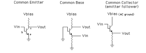
An example of common Emitter
transistor_6
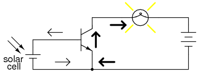
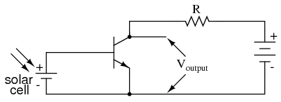
1. Solar cell serves as a light sensor: by using a solar cell to provide 1V (> 0.7V),
  • With the solar cell darkened, the transistor behave as an open switch between collector and emitter.
  • When the solar cell is powered, electrons will flow from the emitter through to the base, up to the left side of the lamp, back to he positive side of the battery —A closed switch
2. Common emitter can e used to produce an output voltage derived from the input signal, rather than a specific output current.
transistor_7 
  • With the solar cell darkened, the transistor behave as an open switch between collector and emitter. there is maximum voltage drop between collector and emitter.
  • When the solar cell is fully powered, minimum voltage drop between collector and emitter.
Note:
  • For an amlifier to work properly, it must be biased on on the time (not just when a signal is present).
    • “On” means current is flowing through the transistor (VB = 0.6 ~ 07V). Usually, a CD circuit is used to achive the biasing.
Common emitter:

Circuit Basics (2)– transistor

Bipolar transistor consists of two PN-junctions — two diodes back to back.
How it works: when you apply a small current to the base (from emitter to base, for NPN type), a much larger current can flow through the transistor (from emitter to collector, for NPN type)
3 leads/legs:
  • emitter,
  • base,
  • collector.
    • One of them is usually grounded.

transistor_1

transistor_2

The choice between NPN and PNP is really arbitrary: all that matters is that the proper current directions are maintained.
Some rules:
  • To get transistors to work,
    • For NPN, collector must be more positive in voltage than emitter.
    • For PNP, collector must be more negative in voltage than emitter.
  • IB + IC = IE,
    • IC is almost equal to IE, as the base current is very small.
  • IC = bIB, b is called the current gain, typically 20 ~ 200
    • Base(small) current is the only current that goes through the base wire of the transistor.
    • Collector(large)current is the only current that goes through the collector wire of the transistor.
    • emitter current is the sum of the base and collector current.

Circuit bacics (1)– Diode

diode

Diode blocks current in one direction while letting current flow in another direction.
 junction diodes are common: put a pice of N type silicon next to a piece of P type silicon.
  • N material has excess negative charge (electrons);
  • P material has excess positive material (holes).
Characteristics:
  • Diode is forward biased when Vanode > Vcathode (usually 0.7Volts, needed to start the hole-electron combination process at the junction).
    • Conducts current strongly.
    • Voltage drop across diode is (almost) independent of diode current.
    • Effective resistance (impedance) of diode is small.
  • Diode is reverse biased when Vanode < Vcathode.
    • Conducts current very weakly (perhaps 10 microamps)
    • Diode current is (almost) independent of voltage, until breakdown (the junction breaks down and lets current through if you apply enough reverse voltage).
    • Effective resistance (impedance) of diode is very large.
Useful links:

IPC:signal basics(3)

Example of signal thread/signal handler

In main thread and other threads,

sigset_t sigset;

sigfillset(&sigset);

sigdelset(&sigset, SIGSEGV);

pthread_sigmask(SIG_BLOCK, &sigset, NULL);

in main thread,

signal(SIGSEGV, clean_up);

if(sigsetjmp(env, 1) != 0) {

          // do something

          exit(EXIT_FAILURE);

}

in signal thread,

sigset_t sigset;

sigfillset(&sigset);

sigdelset(&sigset, SIGSEGV);

pthread_sigmask(SIG_BLOCK, &sigset, NULL);

for(;;) {

if (sigwait(&sigset, &signo) == 0) {

                    // do something;

          }

}

In clean_up(signo)

Option 1 (simple signal handler):

// do something

signal(signo, SIG_DFL);

raise(signo);

option 2(siglongjmp):

signal(signo, SIG_DFL);

siglognjmp(env, 1); 

Note:

  1. signal_thread is not able to catch SIGSEGV, generated due to program errors (it targets to the erroneous thread itself).
  2. signal handler is asynchronous, therefore, inspection and manupulation of shared variables need to be protected.
  3. signal handler is possible to be executed by any thread.
  4. the code after siglongjmp will be continue executed by the same thread which calles signal hander..but the code is a part of main thread..
    1. I have seen an extra SIGSEGV generated, if it is other thread, not main thread, executes the content in sigsetjmp().
  5. even the internal mutex, used between threads, is locked prior SIGSEGV is generated. signal handler, or the code in sigsetjmp can still accquire the mutex, without errors (pthread_mutex_lock() returns 0, no errno set)…the mutex is with default atrributes, no recurrsive. qnx doc says the behavior is unpredictable…

two naive errors

Two pieces of fundamental knowledge:

  1. A local variable with the same name takes preference over the global variable, inside the function/block where the local variable is defined. The same applies to the function parameters.
  2. When program crashes with signo 11 (SIGSEGV), examine core dump by gdb, to locate where the crash occurs.

However, it took me a few hours before realizing it… I was so scared at signal handling,

case 1: The pointer to a context was defined as a local variable in main(). Now, we want to change the context in signal thread/signal hander, two methods:

  • Pass the pointer as an argument when call pthread_create(). // don’t work for signal handler; don’t work for the situation that that the pointer might change (context being destroyed and re-created).
  • Move the pointer declaration out of main().

so, I use the 2nd method. however, I made a mistake, leaving the old local variable still there. you can imagine, every time, when a signal is caught, the pointer is NULL.

I think, …It must be related to signal handling, maybe it is incorrect to share the pointer between signal handler and thread, this way..

 case 2:

 In signal handler of a customized app, it does something, then SIG_DFL(signo). The usual way is signal(signo, SIG_DFL). As the complier doesn’t complain, I think it is the other way to take the default action.

Will SIGBUS lead to a SIGSEGV? I didn’t find a proof while looking at the kernel code, then turned to a collegue.

he asked: what did GDB say?

I: Do you mean using GDB to trace the signal? How?

he said: At least, GDB can tell you where it crashes. where it crashes, does it say the “ip”?

 I realized I need treat it as a normal crash.. then it is so easy, as the system prints ” run fault pid xx tid xx code q ip 0″. it is obvious that the app was trying to access address 0, which is invalid.

the definition of SIG_DFL in signal.h,

#define SIG_DFL             ((void(*)(_SIG_ARGS))  0)